|
Course Module for PCB Design
|
|
INDUSTRIAL TRAINING ON PCB DESNIGN
|
|
PROGRAM DETAILS:
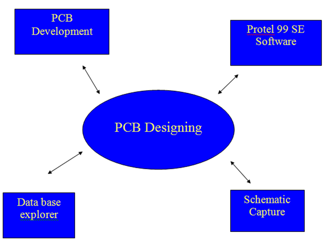
This training will help you to be a part of Electronics Project Team and those who are involved in Electronics Projects All Alone. PCB Design course may help you to get a better JOB opportunity and JOB switchover. There are different programs available in Industrial Training in PCB Design. Students can choose the programs they are inclined to pursue.
| Title |
Module |
Lab |
| PCB design process |
|
- Introduction of PCB Design
|
| PCB Editor workspace |
- PCB Material.
- Using the PCB Editor panel.
- PCB Editor Preferences.
- Board Options dialog.
- Board Layers and Colors.
- Grids.
|
- Introduction ofor cad tool and manufacturing process
- Schematiccreation.
- Symbol creation
|
| Browsing footprint libraries |
- Introduction to Library Design.
- IPC standards in Foot print design.
- Pad Design.
- Foot print design.
|
- Introduction of tools.
- Footprint creation.
- IPC standards.
|
| Creating a new PCB. |
- Creating the Blank PCB.
- Defining a sheet template.
- Defining the Board Shape & Placement Boundary.
- Exercise – Creating a board outline & placement / routing boundary.
|
|
| Transferring design information to the PCB.
|
- Design synchronization with schematic tool.
- Resolving synchronization DRCs.
- Design transfer using a Net list.
- Exercise – Transferring the design
|
- Schematic DRC.
- Bill of material.
- Net list.
- Basic steps for layout.
- Guidelines of layout.
|
| Setting up the PCB layers. |
- Enabling Layers.
- Layer definitions.
- Defining the Electrical Layer
- Defining Mechanical layers.
- Defining PWR/GND layers.
- Exercise – Setting up layers.
|
|
| Design rules and design rule checking |
- Adding design rules in constraints manager
- Design rules concepts.
- How rules are checked.
- Where rules apply.
- Constraint region setting
- Exercise – Setting up the design rules.
- Design Rule Checking
|
- Constraint settings.
- Electrical.
- Physical.
- Spacing.
- Same net spacing.
- Design rules check in pcb
|
| Component Placement tools. |
- Placing components.
- Finding components for placement.
- Moving components.
- Interactive Placement commands.
- Re-Annotation.
- Placement Considerations – [Mechanical – Thermal – Electrical – Assembly].
- Exercise – Component Placement.
|
- Guide lines of placement.
|
| Routing |
- Routing topologies and PCB Routing Considerations.
- Single Ended.
- Differential routing ( Design Considerations).
|
- Routing types.
- Routing guidelines.
- DRC (Design Rule Check)
|
| PCB Layout and Grounding. |
- Discontinuities and other higher order mode effect – bend, vias, pads, connectors.
- Basic layout rules.
- Basic grounding rules.
|
|
| Shielding. |
- Shielding Effectiveness.
- Shielding Practices.
|
|
| Output Generation and Documentation |
- Creating a new Output Job file.
- Setting up Print job option.
- Setting up Print job options.
- Creating CAM files.
- Running the Output Generator.
- Drawing Requirements.
- Assembly Drawing.
- Master Drawing.
- Exercise – adding an Out Job file to the project.
|
|
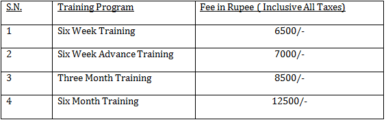
Duration & Program Fee* (Rs):
Project work starts along with the training!
TOOLS:
-
PROTEL 99 se
-
CAMTISTIC 2000
BENEFITS FOR THE STUDENTS
-
Be familiar with the computer aided design software package.
-
Be capable of using the software to produce a schematic and layout diagram from a given circuit diagram.
-
Be familiar with of the relevant industrial process to transfer the design to a copper clad board and produce a bare printed circuit board.
-
It develops an awareness of the various finishing processes involved in producing the finished PCB.
-
Enhances the Skill-Set in your resume for better placement in Electronics Industry.